All of our most skilled space capabilities depend ultimately on an object such as this.
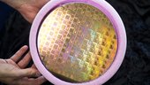
Carefully wrapped in protective anti-static and anti-shock foam packaging, this silicon wafer etched with integrated circuits for space missions was manufactured in an identical batch of 25, worth well over €2 million.
This 20 cm-diameter wafer contains 35 replicas of five different space chips, each one incorporating up to about 10 million transistors or basic circuit switches.
Laid down within a microchip, these designs endow a space mission with intelligence, and the ability to perform various specialised tasks such as data handling, communications processing or attitude control.
To save money on the high cost of fabrication, various chips designed by different companies and destined for multiple ESA projects are crammed onto the same silicon wafers, etched into place at specialised semiconductor manufacturing plants or ‘fabs’, in this case LFoundry (formerly Atmel) in France.
Once tested for functionality, the chips on the wafer are chopped up and packaged for use, then mounted on printed circuit boards for connection with other microelectronic components aboard a satellite.
Since 2002, ESA’s Microelectronics section has maintained a catalogue of ‘building blocks’ for chip designs, known as Intellectual Property cores, available to European industry through ESA licence. For more information, check here.